Landmarks and Research activities
As a landmarks, the involvement that led to establish the first Portuguese partnership with the Nature group, from which it results in the launch of the npj 2D Materials applications journal in 2016. Apart from that I have also to highlight my involvement that lead to the acceptance of FCT-UNL as a core partner of the Knowledge and Innovation Community (KIC) for Raw Materials of the European Institute of Technology, belonging to the Central Colocation Centre, Metz, Germany, 2016. This is a milestone of great relevancy for FCT-UNL and Portuguese strategy.
Apart from that, it should be also highlight that as representative of the European Materials Research Society in the Initiative for Science in Europe (ISE), I participated in the launch activities of the European Research Council, under the Chair of José Mariano Gago (Creating a European Research Council. Letter to the editor, Science, August 2004. http://www.initiative-science-europe.org/pdf/04-Science-Letter-Creating-ERC.pdf). Moreover, I also organised the meeting in January 11th 2007 where Federico Mayor took over as the next ISE Chair, year where Commissionaire Janez Potočnik signed and turn effective the creation of the European Research Council.
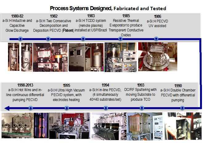
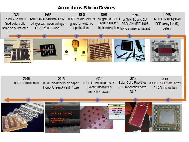
Prior researching oxides and paper electronics, I was involved in the R&D of a-Si;H and a-Ge:H and using PVD techniques, for PV and microelectronics, as position sensitive detectors (psd), thin film transistors (TFT), color detectors and gas sensors (1975-). I started researching oxides as transparent conductive oxides (TCO) for sensors and solar cells, with strong success. Prior I setting up the first clean room for R&D and teaching purposes that took more than one decade (1986-1996), since we start from “ashes”! With this we broad our field of R&D to which strong contribute highly motivated young scientists working under my leadership, allowing us to diverse and to implement research. Going deeply in the understanding of the properties of very thin film oxides (<1 µm) and with the advent of nanotechnologies, we discover that oxides in the range of nm thick exhibit performances by far better than the ones in the bulky, allowing them to be used as real semiconductors. Moreover, they could be deposited at RT. This enabled us to produce the first TFT completely done with oxides (gate, channel, drain, source and dielectric), which catapulted us to the forefront in science and technology. We select ZnO to be a green material and the internal knowledge technology: rf magnetron sputtering. As we could achieve by far the best-reported electronic performances in such TFT processed at RT opening all the possibilities to use low cost flexible substrates for a wide range of applications. Out of this I have to highlight a joint patent done with SAMSUNG.
My current interests are in the design of multifunctional materials, fabrication, transport mechanisms and characterization of amorphous multicomponent oxide TFTs (n- and p-type, the heart of CMOS circuits), exhibiting high electrical mobility’s for paper electronics. Furthermore recent progress in nanotechnology provides a new approach to develop active functions in oxides and paper: (i) use of natural nanostructures embedded oxides and (ii) fabrication of artificial nanostructures assisted by nanolithography techniques and new femtosecond laser processing. As European I want to be in the leading edge of this research frontier to which I would like to bring the features of paper electronics as something born and matured in Europe from which Europeans will profit in a medium long term range, since intense research is required, going from the understanding of the physics and chemistry behind the nano-materials components to devices and systems that aim to develop to turn viable the industry use of them. To this dream my past proves that we can do it! The word “impossible” do not exist in our dictionary.
My main achievement as far conducting research and high level formation is concerned relies on having formed and having work with me 4 ERC awards: Elvira Fortunato, my PhD student and my co-worker, got an Advanced ERC Grant in Materials Science and Engineering (Advanced Amorphous Multicomponent Oxides for Transparent Electronics, Invisible, 2.25 M€) in the first edition (2008); I. Ferreira my PhD student and my co-worker, got in 2015 a consolidator ERC grant in Materials Science and Engineering ("Integration of capacitor, thermoelectric and photovoltaic thin films for efficient energy conversion and storage"- CapTherPV., 2 M€); Luis Pereira a start ERC grant in Materials Science and Engineering "New era of printed paper electronics based on advanced functional cellulose - NewFun", 1.5 M€); Pedro Barquinha, my co-supervisor student and member of my team, got in 2016 a start ERC grant in Materials Science and Engineering (“Transparent and flexible electronics with embedded energy harvesting based on oxide nanowire devices- TREND , 1.5M€)”.
Below see the landmarks of my activity in the 5 core topics of: Process Systems design, fabrication and testing; amorphous silicon solar cells; Transparent Electronics, Paper Electronics; Electrochromics and microelectronics.
(landmarks_5_core_topics_professor_rodrigo_martins.pdf)

Keywords
• Design, testing and manufacturing of process deposition systems
• Transparent electronics
• Paper Electronics
• Thin film transistors
• Metal oxide semiconductors;
• Flexible Solar cells;
• Solar Roof tiles;
• Plasmonics
• Thin films
• Microelectronics
• Biosensors
• Nanotechnology