Manuel J. Mendes Website
Professor of Photonics, Photovoltaics and Optoelectronics subjects
CENIMAT-i3N and CEMOP-UNINOVA, Faculdade de Ciências e Tecnologia, Universidade Nova de Lisboa. Campus de Caparica. 2829-516 Caparica. Portugal (email)
CENIMAT-i3N and CEMOP-UNINOVA, Faculdade de Ciências e Tecnologia, Universidade Nova de Lisboa. Campus de Caparica. 2829-516 Caparica. Portugal (email)
| The Nanophotonics and Energy lab headed by Prof. Manuel J. Mendes is part of the MEON group of CENIMAT-UNINOVA and is dedicated to advancing knowledge and technology in the frontline of Photovoltaics (PV). | |
| Our team has strong interest in modelling, characterization and fabrication of nanostructured materials and devices, in order to demonstrate novel PV concepts, in particular being world pioneer in photonics and quantum structured solar cells, as well as in thin-film PV integrated on flexible substrates. |
Location: Lab 2.1.18 in CEMOP building |
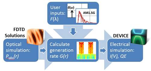
At the Nanophotonics & Energy team one of our main expertise is in Light Management for PV, namely:
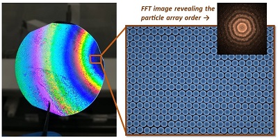 |
Example of a micro-structured sample optically analyzed in the lab. The left photo shows a 2-inch c-Si wafer coated with a self-assembled array of colloidal particles, which is used as patterning mask to engineer photonic structures in solar cells. The right SEM image is a top-view of the colloidal monolayer, whose long-range ordering is shown by the processed Fast-Fourier Transform (FFT) inset image. The high periodicity of the deposited array makes it act like a diffraction grating, resulting in the strongly bright rainbow of colours visualized in the photo. Colours originating from micro-structuring are also found in several natural constructions, such as in butterfly wings, peacock feathers, among a myriad of other examples. |
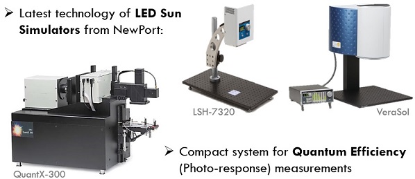
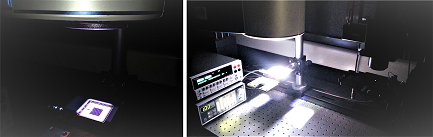
The group counts with outstanding facilities, installed in CENIMAT-CEMOP, for pursuing the R&D activities, namely: